S-Cam 2
Introduction
| This page has been archived and is no longer updated. |
S-Cam 2 was the second prototype of a cryogenic camera for ground-based astronomy, based around a 6×6 array of Ta-Al STJ's. S-Cam 2 was an improved version of S-Cam 1, which was tested on the William Herschel Telescope in La Palma (Canary Islands) in early 1999. S-Cam 2 was used on three successful observing campaigns on the same telescope in December 1999, April 2000 and September/October 2000. Work is now advanced on S-Cam 3, a completely new instrument incorporating many technological improvements, including a larger array with 120 pixels. It is intended that S-Cam 3 will see first light in the latter quarter of 2003. Most of the technical information on these pages currently relates to S-Cam 2.
The STJ Detector Array
Ta-Al STJ's have high responsivities, high detection efficiencies (~70% in the visible), adequate resolving power (~10 at 300 nm) and very fast response times (on the order of 10 microseconds). After testing different configurations, the array chosen for S-Cam 2 consisted of 36 diamond-shaped 25 micron devices, with a spacing between pixels of 4 microns. The detectors are fabricated from an original Ta-Al-AlOx-Al-Ta multilayer, deposited by sputtering onto a highly polished 520 micron-thick sapphire substrate. The thick aluminium layer gives S-Cam 2 a higher responsivity than its predecessor, which - coupled with improved IR rejection - resulted in an enhanced signal-to-noise performance. More details about the fabrication process may be found in Rando et al 2000.
 |
|
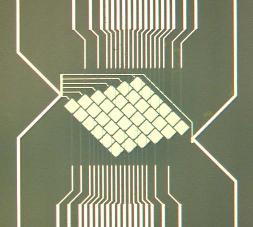
Optical microscope photograph an S-Cam6×6 Ta array, in this case with 40 micron pixels. The wiring connecting the base and counter electrodes to the external pads is clearly visible, as well as the path of the return lines. |
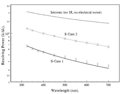
The resolving power of the array as a function of wavelength represents a considerable improvement over S-Cam 1, although it is still some way below the intrinsic resolving power which would be expected in the absence of IR contamination or electrical noise. Contributions to the degradation in the resolving power in the actual array include spatial non-uniformities in the detector responsivity, noise in the Front-End electronics and by statistical fluctuations in the background radiation - essentially IR radiation originating from objects close to or in the field of view of the detector.
 |
|
The resolving power of a typical S-Campixel. The dashed line is the theoretical resolving power. Note the improvement between S-Cam 1 and 2. |
The STJ Detector Array
| This page has been archived and is no longer updated. |
The S-Cam 2 detector array was read-out by means of 36 Charge Sensitive Preamplifiers, one for each pixel, and a related shaping stage, all taking place at room temperature. The amplitude and risetime of the detected pulse corresponded to the total collected charge and to the decay time of the signal respectively. Noise is assessed by measuring the FWHM of the peak distribution generated by an electronic pulser.
 |
|
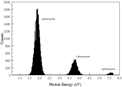
Figure 1: Charge spectrum obtained by a single pixel (4,4) with the array illuminated by a pulsed led (red; 630 nm) when integrated into the S-Cam 2 cryostat and undergoing system tests. The additional peaks are due to multiple (n=2 and 3) photon events. |
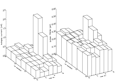
The integrated system test conducted prior to shipment to the William Herschel Telescope confirmed good reproducability of the electrical characteristics of the array, and also demonstrated that it was possible to operate all pixels at the same bias voltage (about 200 microvolts, typically) and with uniform responsivity. The typical pixel-to-pixel responsivity variations were at the 5 % level. As shown below, three pixels had substantially higher subgap currents than the rest of the array. The cause of this non-uniformity is not fully understood, but is suspected to be due to the IR background as seen by the individual detectors, rather than any intrinsic array defect. The larger FWHM obviously leads to a lower S/N and thus worse resolving power. Fortunately the pixels in the center of the array, where the stellar image was likely to fall, were well-behaved.
 |
|
Figure 2: 3D histograms of the subgap current at the bias voltage and of the corresponding test-pulse energy resolution for all elements of the array. Pixels (5,2), (5,3) and (5,4) show larger subgap currents and worse energy resolution. |
The Cryogenic Camera
| This page has been archived and is no longer updated. |
The characteristics of the camera are summarised in the table below. The main improvements implemented in S-Cam 2 concern the increased resolving power (now ~8 at 500nm), the higher maximum count rate sustained by each of the electronics channels (now 5 KHz per pixel), the simplified alignment procedure, and a number of improvements in the Graphical User Interface (GUI) software. The camera design is based on a bottom loading 4He cryostat hosting an adsorption ³He cooler. A dedicated optical collimator unit interfaces the camera focal plane to the Nasmyth focus of the Ground High Resolution Imaging Laboratory of the William Herschel Telescope, in La Palma.
A plate scale of 0.6 arcsec per pixel was selected to match the telescope point spread function, which is typically around one arcsec. The optical unit is based on a reflective section and on a lens objective. Two filter wheels are available with neutral density and narrow band filters. The neutral density filters are needed to hold down the count rate for bright objects (such as flux standard stars) which would otherwise exceed the 5Khz per pixel maximum event rate of the array. The front-end electronics is based on 36 charge sensitive preamplifiers and related shaping stages operating at room temperature. These permit pixels to be biassed and read-out individually. Each channel has a peak detection unit and an analog-to-digital converter, allowing pulse-height analysis to be performed on every detected photon. Accurate time-tagging of these events is crucial, and is achieved using a commercial GPS receiver with an accuracy of ~ 5 microseconds. The electronics system is connected to a dedicated data acquisition computer, which is in turn connected to the control PC on which the GUI is run. This PC would typically be operated from within the telescope control room. Data storage takes place on the same unit.
| Band-pass: | 350-650 nm (at 10% photon collecting efficiency) |
| Data per detected event: | Wavelength, arrival time, pixel # |
| Resolving power: | of order 10 at 300 nm |
| Event time resolution: | 5 microseconds (GPS) |
| Maximum count rate: | 5 kHz/pixel |
| Camera field of view: | 4.0 × 4.0 arcsec |
| Instrument installation: | Nasmyth focus (f/11) - WHT |
| Observation time: | In excess of 10 hours (cooler hold time) |
| Camera focus adjustment: | Telescope secondary mirror and dedicated optical unit |
| Camera Guiding: | Telescope facility (autoguider camera) |
| Filter wheel: | 2 sets of 8 filters on 2 independent wheels |
| On-line data analysis: | 'Quick-view' SW on control PC |
| Data storage format: | FITS format (via control PC) |
Because the detector has such high responsivity and detection efficiency, it is crucial to reject thermal infrared photons if the resolving power of the instrument is to be optimised. The expected sky background flux at the Nasmyth focus is not a major problem (producing about 50 counts per second per pixel), but the thermal radiation emitted by warm components in the field of view has a major degrading effect on the system performance. To counter this, S-Cam 2 uses two KG2 glass filters of different thicknesses, cooled to 12 and 2 K respectively. A third silica element is located in front of the focal plane array and maintained at 0.32 K. The optical entrance window of the cryostat is sapphire, with standard ARC's on one side and a multilayer IR filter on the other. These filters reduce the overall camera throughput in the nominal band-pass to about 25%. Further work is on-going to improve the efficiency of the IR filters.
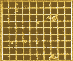 |
|
One possible solution to the IR contamination problem lies in the development of blocking grids. This 9×10 prototype grid was milled from a gold-coated sapphire chip using a focussed-ion beam. The grid bars are 100 nm wide. |
Results: Crab Pulsar
| This page has been archived and is no longer updated. |
 |
|
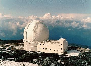
The 4.2m William Herschel Telescope, situated at the Observatorio de Roque de los Muchachos, at an altitude of 2330 m, on the island of La Palma in the Canary Islands. |
The first test campaign with S-Cam 1 took place in Jan-Feb 1999. Although observing conditions were poor, the basic viability of the instrument was demonstrated, paving the way for three more runs which have since taken place with S-Cam 2. In particular, the unique timing and energy resolving capabilities of the instrument were demonstrated by observing the Crab pulsar (see below):
 |
|
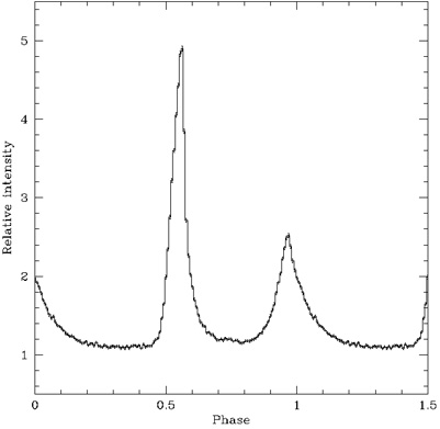
Pulse profile of the 30 millisecond Crab pulsar, obtained with S-Cam 1 on 6 Feb 1999. The data spanned 310-610 nm and were obtained over a period of 50 minutes. |
S-Cam 2 went to the mountain in Dec 1999, April 2000 and September/October 2000, with only small technical changes made between the three runs. In all instances the observing conditions were satisfactory. The three campaigns focussed on astronomical exploitation of the camera, rather than on engineering aspects, and a choice of observing targets was made with particular care to utilise the instrument's unique capabilities. Among the objects looked at in all three runs, for instance, were a number of cataclysic variable (CV) stars. CV's are binary stars containing a white dwarf and a normal star, and are typified by short orbital periods and rich temporal and spectroscopic behavior. Eclipsing CV's are particularly interesting since the rapid colour changes seen during the ingress and egress of the eclipse is dependent on the geometry of the various components in the binary - stars, accretion streams, hotspots etc. S-Cam 2's rapid time variability and moderate energy resolution is ideally suited to studying these phenomena.
Results: Cataclysmic Variable
|
Artist's impression of a polar, a magnetic cataclysmic variable. Picture used with permission of Mark A Garlick. |
As an example of what can be obtained, data from the CV UZ For are shown here. This is one of a class of short-period CV's known as polars or AM Her stars. The two stars which constitute the binary are very different: a low-mass dwarf star cooler than our sun but which is still burning hydrogen in its core, and a much smaller stellar remnant known as a white dwarf. White dwarves - the evolutionary end-point of a sunlike star - typically contain about as much mass as our own sun, but squeezed into a volume about the size of the Earth. In the case of polars, they are also highly magnetized, with surface magnetic field strengths ranging from 10 to 70 MG. The two stars are so close that they may orbit around each other in only a few hours, with matter being drawn off the ordinary dwarf onto the surface of the white dwarf, giving off X-rays in the process. The white dwarf rotates synchronously with the binary period and its strong magnetic field prevents the infalling matter from forming an accretion disk.
 |
|
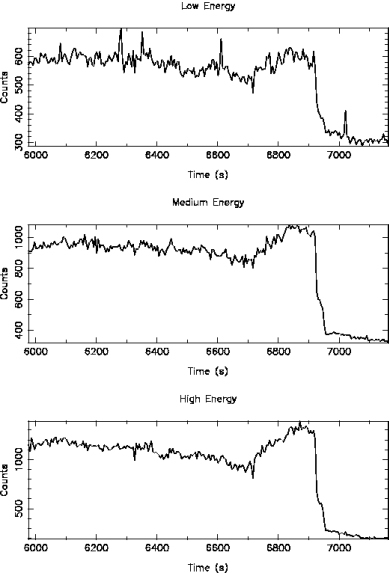
Light curves in three separate energy bands for the eclipsing binary UZ For. Note the ledge-like structure in the eclipse ingress (most clearly seen in the high energy data); the sharp initial fall, followed by the ledge, can be interpreted as evidence of two hotspots near the white dwarf. |
Results: Eclipse UZ Fornax
| This page has been archived and is no longer updated. |
In order to demonstrate the capabilities of S-CAM 2, we have created an animation showing an observation of an entire eclipse of UZ For. This was created by splicing together two integrations, with the join between them near the mid-point of the eclipse. Each step in the animation corresponds to 3 seconds of actual data.
The lightcurve in the top of the plot shows the evolution of the total source intensity across the complete spectral range. In order to illustrate the energy-sensitivity of the device, however, the 36 array pixels in the lower image are first assigned colours based on the V/R ratio obtained from two energy bands (ranging from blue to red on a spectral scale), and are then assigned intensities based on the total counts in that pixel over the 3 second time period.
 |
|
For more information on this observation, see Perryman et al 2001. |
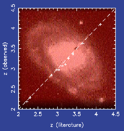
A number of other cataclysmic variables have also been the subject of S-Cam 2 studies, including HU Aqr (Bridge et al 2002), Ep Dra (Bridge et al 2003) and IY Uma (Steeghs et al 2002), with more data still be to be analysed. Other studies have shown that S-Cam 2 is a powerful instrument for making direct measurements (without dispersive optics) of both quasar redshifts (de Bruijne et al 2002) and stellar temperatures (Reynolds et al 2003).
 |
|
The redshifts of eleven quasars, as determined by direct spectral fitting to S-Cam 2 data, versus the literature redshifts of the same eleven objects. |
References (published S-Cam studies):
Perryman M.A.C., Cropper M., Ramsay G. et al 2001 MNRAS, 324, 899
Bridge C.M., Cropper M., Ramsay G. et al 2002 MNRAS, 336 1129
Bridge C.M., Cropper M., Ramsay G. et al 2003 MNRAS, 431 863
de Bruijne J.H.J., Reynolds A.P, Perryman M.A.C., 2002 A&A, 381, L57
Reynolds A.P., de Bruijne J.H.J, Perryman M.A.C., 2003 A&A, 400, 1209
Results: Time-resolved Crab animations
| This page has been archived and is no longer updated. |
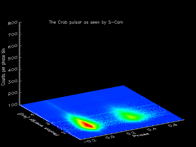
During the S-Cam 2c campaign, a number of observations of the Crab pulsar were made. The pulsar is an isolated neutron star that rotates 30 times a second, sending out two "lighthouse beams" of radio and optical emission from the star's magnetic poles. When these sweep over us we see two pulses - one of which is more intense than the other. S-Cam's timing capability enables the pulse profile to be recorded, but we can also display the variation in emission with energy, as illustrated below. The animation below shows the pulse profile building up as we move forward in phase.
Click on the image to play the animation
 |
900 s of data were used to create the animation, folded on the period of the Crab and divided into 335 phase bins. The data were binned into 255 PHA (or energy) bins, of which only those from 50 - 210 are plotted, corresponding to ~ 1 to 5 eV. Intensities (counts per phase bin) are colour-coded. The sky background spectrum has been subtracted.
For best results, it may be best to play the movie more than once.
Results: Time-sliced Crab animation
| This page has been archived and is no longer updated. |
Here is another animation of the Crab, this time showing a moving slice through the pulse profile as we move forward in phase.
Click on the image to play the animation
 |
900 s of data were used to create the animation, folded on the period of the Crab and divided into 335 phase bins. The data were binned into 255 PHA (or energy) bins, of which only those from 50 - 210 are plotted. Intensities (counts per phase bin) are colour-coded. The sky background spectrum has been subtracted.
For best results, it may be best to play the movie more than once.
Results: Phase-resolved Crab animation
| This page has been archived and is no longer updated. |
Here is another animation of the Crab, this time showing the phase-resolved image.
Click on the image to play the animation
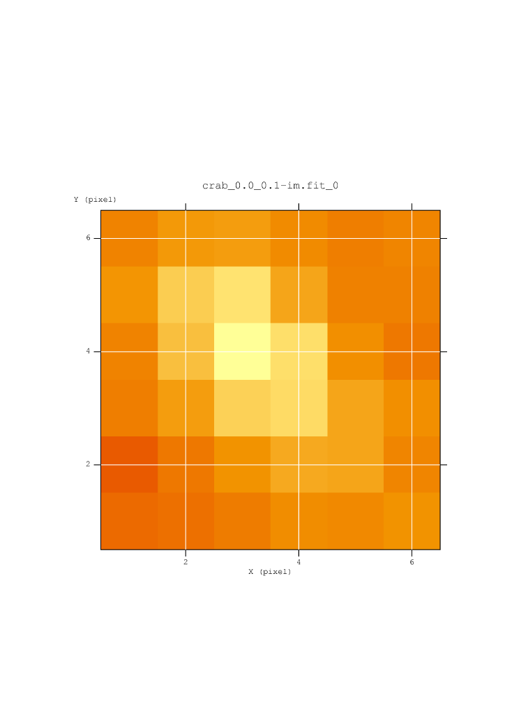 |
3 s of data were used to create the animation, spanning ~ 90 pulse cycles. The data were selected into 10 phase bins, and the animation consists of one averaged pulse cycle shown five times. The main and secondary pulses are clearly seen, as well as the drop to low intensity between the pulses. The phasing is arbitrary.
For best results, it may be best to play the movie more than once.