S-Cam 3
- Increase the field-of-view from 4" × 4" to 11" × 9"
- Optimize IR rejection filters, possibly extending the 'red' response towards ~1μm
- Increase the energy resolution
- Increase the electronics readout speed and hence the system's photon rate capability
- Improve the data acquisition software's robustness
The Detector
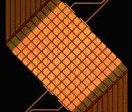
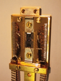
The first objective was met by a redesign of the detector. The S-Cam 3 detector is an array of 10 × 12 pixels each 33 × 33mm² with 4mm interpixel gaps. The increased pixel size corresponds to ~0.8" × 0.8" on the sky. The large increase in the number of pixels and the moderate increase in pixel size have increased the field-of-view of the instrument from 4" × 4" in S-Cam2 to 11" × 9" in the new instrument. This ensures uncompromised photometry on point sources, even under poor seeing conditions and more accurate background subtraction. Also simultaneous imaging of more than one object becomes possible, which is useful when observing extremely weak objects. Figure 1 and Figure 2 show micrographs of the S-Cam 3 array.
 |
 |
|
Figure 1: S-Cam 3 array; 10×12 pixels each 33×33 μm² |
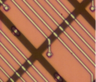
Figure 2: Detail showing Nb contacts and plugs |
The array is divided in 4 electrically separated subarrays of 10×3 pixels. All 30 pixels in a subarray share a common return wire connected to the base electrodes. The base electrodes are therefore interconnected in colums of 10 pixels and the 3 colums to a single return contact (see figure 5). The pixel interconnects ('plugs') are made out of Nb to inhibit signal cross talk due quasi-particle diffusion from one pixel to the next (see figure 6). The blocks of 30 pixels are matched to the modular setup of the readout electronics, which consists of 32-channel sub-units.
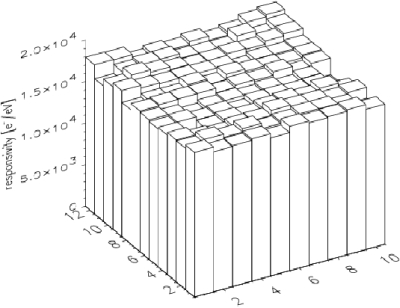
The layup of the detectors is identical to the S-Cam2 arrays: 100nm Ta with 30nm Al trapping layers. The best arrays shows 100% pixel yield: all 120 pixels are low-leakage STJs with typical leakage currents of ~30pA. The responsivity (defined as the total collected charge in electrons per electron-Volt of incident photon energy) for the selected array is slightly increased from ~15000e-/eV in S-Cam2 to ~18000e-/eV in the current devices. Figure 3 is a responsivity map of the same device, illustrating the full functionality of the chip as well as the uniformity across the array.
|
|
|
Figure 3: Responsivity map. For each pixel of the array, the total collected charge in electrons per electron-Volt incident photon energy is plotted. 1σ deviation is <3.3% |
With these effects combined, we have been able to measure a resolution R=13 at 500nm, up from R=8 in S-Cam2.
Figure 9 shows a picture of the detector chip mounted on the cold finger. Unfortunately, this detector chip suffered major damage due to electrostatic discharge in the course of the S-Cam 3 final assembly. As a result 45 pixels were lost entirely, while some others suffered from degraded responsivity and resolving power.
The rejection of thermal infrared photons is of crucial importance. The low energy gap of Ta/Al STJs makes them sensitive to wavelengths up to ~1mm. Since the detector is optically coupled to a 300K environment, the IR rejection filters have very tight requirements. In S-Cam2 this problem was solved by baffling and by using Schott KG2 and KG5 glasses. Simple calculations of attenuation factors in the vicinity of the peak of the 300K blackbody radiation could, however not explain the excess in sub-gap current measured in S-Cam 2. We concluded that we were suffering from residual very long wavelength radiation. In order to optimize the suppression of the longer wavelengths, while maintaining high throughput in the visible, the KG5 glass was replaced by 2 BK7 windows (each 9.5mm thick, one at 4K the other at 0.3K). This, in combination with improved baffling and shielding, reduced the IR load per unit detector area by more than an order of magnitude. Figure 10 shows a picture of the detector assembly, including the signal wiring and one of BK7 windows.
The sapphire entrance window is now coated with an anti-reflection coating rather than an IR reflection coating.
 |
|
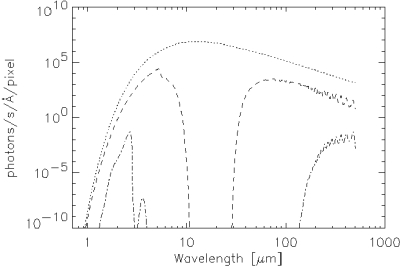
Figure 4: Dotted curve is the photon flux from a 300K black body radiator. Dashed curve is remaining photon flux from 300 K BB passing through the detector's sapphire substrate. Dot-dashed curve is remaining 300K BB flux passing through S-Cam 3 optical path (IR filters + substrate) |
 |
|
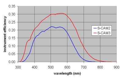
Figure 5: Comparison of the overall detection efficiencies of S-Cam 2 and S-Cam 3 |
Figure 5 is a comparison of the total efficiency of S-Cam 2 versus S-Cam 3. These curves take into account the measured transmissions of all optical elements as well as the detector's efficiency. The peak efficiency has increased from ~22% in S-Cam 2 to ~30% in S-Cam 3. The bandwidth (at 10% of maximum) has also increased from 335–690nm to 330–745nm.
The Readout Electronics Architecture
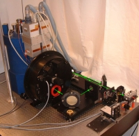
The S-Cam 3 electronics is still based on discrete components. The input amplifiers are grouped in sets of 32 channels in individual housings. A set of four boxes (128 channels in total) is mounted directly on the cryostat (see figure 6). The input stage of the preamplifiers consists of JFETs in a cascode configuration. The amplifiers' buffered differential outputs are routed through a few meters of twisted shielded cables to the pulse processing stages.
 |
|
Figure 6: S-Cam cryostat (blue) with 4 preamplifier units (32 channels each) mounted. In the foreground are relay optics and filter wheel |
The preamplifier board also carry circuitry to provide stable low noise voltage biasing of the STJ, offset voltage compensation, and I-V curvetracing to verify the each individual pixel's in situ.
Each buffered preamplifier signal is digitized at a programmable rate of up to 40 Msamples per second. The digital samples are passed to a FIR filter which serves as the shaping stage. By changing the length of the filter (up to 1536 taps) and/or the sampling rate, the effective pulse shaping time can be tuned. This allows to optimize the settings for either speed, with a short FIR (lower pile-up probability) or better energy resolution, with a longer FIR.
The FIRs are integrated into FPGAs, together with functions like threshold detection, peak search and sampling, time tagging, a digital pulse generator for electronic noise determination, buffering and the required glue-logic. Each event, which passes a programmable threshold, will be detected and the pixel address information with a time tag derived from a GPS receiver is forwarded to a fast buffer. The hardware buffer is then readout by a PC using a fast PCI parallel port and logged onto disk.
By separating these the data streams for event logging and GUI/display facilities, and also by performing most of the quick-look processing in hardware (for example, FPGAs accumulate spectra), the speed and robustness of S-Cam 3 has been improved tremendously over S-Cam 2.
The Cryogenic Cooler
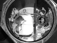
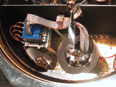
In order to cool the detector to its operating temperature of ~0.3K, we use a dewar in combination with sorption coolers. The dewar can contain ~12 litres of liquid Helium. An inside view of the S-Cam 3 cold plate is given in Figure 7. The coupling to the external optics is on the right hand side. The light will first pass a number of filters before going through the split-pair magnet (circular part to the right) onto the detector, suspended in the center of the magnet. The detector holder is thermally connected via a Cu strap to the ³He sorption cooler.
|
Figure 7: Upside-down view of the S-Cam 3 cold plate. Light enters from the right through a number of IR blocking filters to reach the detector suspended in the middle of the magnet (circular part on the right-hand side). The detector holder is thermally anchored to the ³He sorption cooler, part of the hybrid cooler seen on the left-hand side |
Figure 8: Hybrid Sorption coolers from CEA. The cups are the evaporators of the 4He (right) and ³He coolers (left). The Cu connections around the middle of the vertical stainless steel tubes are the condensers |
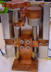
Contrary to S-Cam 2, S-Cam 3 uses a hybrid 4He–³He sorption cooler combination (see figure 6) from the CEA in Grenoble. In principle, the 4He cooler of this system can provide adequate precooling required to condense the ³He, but we found that ³He and 4He condensation were much more efficient when assisted by a lower bath temperature of ~2.5K, achieved by pumping on the He. In this way the hold time at the base temperature of 285 mK is >24 hrs. In combination of ~18 hours hold time of the helium bath this allows for uninterrupted stable operation throughout the night and conventnient recycling in during day.
 |
 |
|
Figure 9: S-Cam 3 cold finger with detector chip |
Figure 10: Integrated detector assembly including one of the BK7 windows |
 | |
|
Figure 11: Detector assembly integrated inside the split pair magnet on the S-Cam 3 cold plate | |
Summary of S-Cam 3 Characteristics
| Detector | 12×10 Ta/Al STJs |
| Pixel size | 33×33 μm² |
| Fill factor | 76% |
| Plate scale | 0.8"/pixel |
| FOV | 11"×9" |
| Pass band | 330-745 nm |
| Maximum detection efficiency (@500nm) | 30% |
| λ/∆λ @ λ=500nm | 8-11 |
| Event time resolution | ~5 μs |
| Max. event rate/pixel | >8000 cts/s |
| Max. overall event rate | ~106 cts/s |
| Max. observation time | 24 h |
| Operating temperature | 285 mK |
First Observing Campaign - July 2004
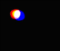
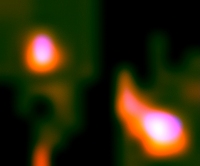
S-Cam 3 saw first light during a 7-night observation campaign at the 4.2 m WHT at La Palma (Spain) in the first half of July 2004. The instrument performed extremely reliable, with only 15 minutes of observation time lost due to instrument failure. The observation programme was focused on the detection of temporal and spectral variability in a number of targets. Data processing and analysis is currently underway. Figure 12 shows a processed image of a point source under fairly poor seeing conditions. Using the detectors intrinsic wavelength resolution, the effect of differential atmospheric refraction is clearly seen. Figure 13 is a processed image of 9"×11" in which 5 different sources can be distinguished, including a galaxy in the lower right part. The star in the upper right part is 19th magnitude. Note that there is some distortion in this image due to the dead pixels.
 |
 |
|
Figure 12: Processed S-Cam 3 image of a 16th magnitude star showing the effect of differential atmospheric refraction |
Figure 13: Processed S-Cam 3 image of a 9"×11" field, showing multiple point sources and an extended source |