The Future of Compound Semiconductors
For gamma-ray applications, the objective should be to produce a detector, that will operate at, or above room temperature, with a fwhm energy resolution of 1% at 500 keV or less and a usable active volume of a cubic cm.
General Requirements
In terms of general requirements, Z should be greater than 40 to yield a high stopping power. Structurally, the lattice should also have a close packed geometry (such as a body centred cubic structure) to optimize density. The material should have a low dielectric constant, to ensure low capacitance and therefore system noise. For practical systems preference should be given to binary or pseudo alloyed binary systems over ternary or higher order compounds, based on the multiplication of stoichiometry errors. Additionally, such a restriction would also "clean-up" the response function by reducing the number of "unwanted" absorption and emission features in the measured energy-loss spectra. The selection criteria can be further extended to exclude most II-VI compounds in view of their propensity for toxicity, deep trapping and polarization effects, coupled with their low melting points. The latter makes it difficult to perform the required thermal annealing to activate implanted dopants.
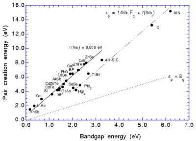
From an electronic point of view, the band-gap energy should be greater than 0.14 so there is no thermal generation of carriers at room temperature and the resistivity should be greater than 108 Ωcm to allow larger biases to be applied, resulting in faster drift velocities and deeper depletion depths. For the highest Z materials, Fano noise can also be substantially reduced (and hence energy resolution improved), by choosing compounds from groups n(period 6)-VIIB, where n=II,III or IV (for example, HgI2). This is illustrated in figure 1 in which the band-gap energy is plotted as a function of electron-hole pair creation energy. From the graph we see that the compounds HgI2, PbI2 and TlBr are clearly displaced from the line describing the bulk of the semiconductors, giving a ~30% reduction in the mean pair creation energy for a given band-gap compared to the main branch. Indeed, if the n(period 6)-VIIB relationship really exists, then BiI3 should also lie on the second branch.
A practical upper limit of ~ 2.2 eV can be placed on the bandgap energy, based on the fact that carrier mobilities tend to drop rapidly with increasing bandgap due to polar lattice scattering. In addition, heavy compounds in this category tend to be mechanically soft or layered making them difficult to handle. Consequently, they do not lend themselves to standard processing techniques, particularly array replication. Finally, electron and hole mobility-lifetime products should be better than 10-2 and 10-3, respectively, to ensure good carrier transport and therefore spectral performance. This in turn, places a limit on the density of typical trapping centres of < 5 × 1012 cm-3. Applying the above criteria reduces the number of acceptable compounds to about ten.
The Longer Term
In the preceding sections we have concentrated purely on material developments. In the longer term, material improvements must be paralleled by corresponding developments in heterostructure and quantum heterostructure technology, provided of course strain is not a limiting factor. Doping a semiconductor like Si or GaAs provides control over the sign and density of the charge carriers. By combining different semiconductors in heterostructures, one gains control over much more, including the band gap energy, refractive index, carrier mass and mobility, and other fundamental parameters. For example, heterostructures may solve the problem of contacting by building up a series of semiconductor layers until it is possible to satisfy the relationship that the workfunction of the metal contact is less that that of the semiconductor (φm
In principal, quantum heterostructures could also facilitate ultra-low noise operation by constructing a series of quantum valleys, which have the dimensions of the order of 0.1 nm at the contact side and millimetres or even centimetres on the intrinsic-layer side. As such, the read-out would have approximately the dimensions of the readout node of a Si CCD, which is directly responsible for their ultra low noise operation. The basis of operation is based on the work of Esaki and Tsu [J. Res. Develop., 24 (1970) 61], who suggested that it would be possible to grow alternating layers of GaAs and AlGaAs in a periodic array to form a super-lattice, which would have remarkably different electronic properties from those of bulk GaAs or AlGaAs. When a layer of GaAs is sandwiched between two "infinite" layers of AlGaAs, the carriers in the GaAs are trapped in the GaAs layer along the growth direction. In this structure, the energy levels in the well are raised in the conduction band for the electrons and lowered in the valence band for the holes. This leads to the confinement of electrons along the growth direction and characterizes the well as a structure that has a 1-D confinement for charged carriers. The composite of many such layers, would form a bi-periodic array of rectangular quantum wires.
At the present time, the first purpose-built heterostructures for X-ray applications are being reported in the literature. For example, Silenas et al. [Nucl. Instr. and Meth., 546 (2005) 228-231] have constructed an n-GaAs - p-AlGaAs graded-gap X-ray detector in which the AlGaAs layer functions as the classical absorption and detection layer and the n-GaAs layer as a carrier multiplication zone. Early results show the device is sensitive to α-particles and gains of up to 100 can be achieved.
Perhaps even more speculative, we note reports of porosity in III-V compounds, particularly, GaAs, GaP and InP [H. Föll, et al., Phys. Stat. Sol. (A), 197 (2003) 61]. While one can envision photonic crystal applications, depending on cytotoxicity, this also leads to the possibility of animal cell:semiconductor interfacing as in the case of nanostructured Si [S.C. Bayliss, et al., J. Mat. Sci. Lett., 17 (1997) 737].


