Optical/UV Detectors: Matrix Readout Devices
Introduction
Micrographs of two 6x6 Tantalum STJ arrays, wired in matrix format (left) and with individual readout (right). Note the increased wiring complexity of the latter.
The division is engaged in the development of a novel readout scheme for large area STJ arrays, which can in principle be applied to other kinds of detector array (see Martin et al 2000 for more details of the work summarised here.) The scheme is intended to do away with the requirement for every pixel in an array to have its own acquisition chain, for the following reasons:
- Current amplifiers with the required energy resolution cannot operate at the detector temperature and so need to be connected to the array with wiring. The wires impose an undesirable heat-load onto the cryogenic cooler.
- For X-ray spectroscopy, illumination has to be through the front or top electrode. The amount of wiring crossing the detectors suppresses the low energy response.
- For space-based instruments, power consumption and weight are to be minimized - precluding the development of large-format arrays in which each pixel has its own biassing circuit and pre-amplifier, shaping filter, low-level threshold detector, sample-and-hold and analog-to-digital converter circuits.
- The method described here necessitates less wires on chip as well as between the detector and the acquisition electronics. It reduces by the same amount the number of electronic channels. In place of N2 amplifier chains that would normally be required for an NxN pixel array, only 2N are needed in matrix format.
Read-out description
The principle is based on interconnecting the pixels in rows and columns. In the specific case of an STJ array, the base electrodes are interconnected in rows and the top electrodes in columns, with each row and column being connected to a separate bias and amplification circuit. This means only 2N wires for NxN pixels. When a photon hits a pixel, it produces a signal in the corresponding row and column. Coincidence measurement between rows and columns can therefore determine which pixel recorded the event. The photon energy is measured in the usual way for an STJ-based device.
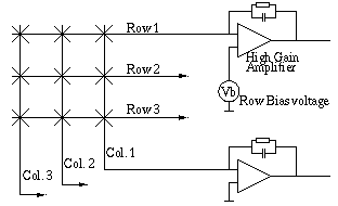
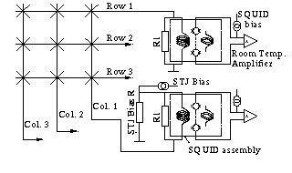
Top: diagram showing matrix array connections to charge sensitive amplifiers. Bottom: matrix array connections to DC-SQUIDS.
The figures above show wiring diagrams for matrix read-out, using JFET charge sensitive amplifiers (top) and SQUID current amplifiers (bottom). In the case of the JFET arrangement, voltage biassing of the detectors is achieved by creating a virtual ground on all columns and a virtual bias voltage on all rows. This can be implemented using a high open loop gain amplifier with negative feedback and avery low offset voltage operational amplifier controlling the amplifier's JFET DC operating point. For the SQUID arrangement, the biassing circuit is greatly simplified. There is also reduced pick-up noise since the SQUIDS are placed close to the detectors and present a low output impedance. Unfortunately current SQUID's cannot be connected to STJ's and so the low-noise level obtainable with the JFET approach is not yet reachable.
Advantages
The matrix scheme opens the way to large format arrays. The conventional approach would limit the number of pixels to about 100, or perhaps 1000 assuming major development in the problem of reducing the heat load on the cryogenic system. With the matrix approach, arrays of 104 or 106 can now be envisaged; ie comparable to smaller CCD arrays. Large field imaging spectrometers would then become available for UV-Optical and X-ray astronomy.
Since the number of connections to the detector chip has decreased and because the contacts are intrinsically available at the border of the array no complex routing is needed to connect the array pixels to the reduced number of contact pads. Bonding to the chip can be achieved by traditional wire bondingm, with no bump-bonding being necessary.
The traditional method requires a separate top electrode contact for each detector and therefore the number of tracks required increases rapidly with array size. The tracks covering the top electrodes mask the detector in the case of top illumination, which becomes unacceptable for larger arrays.
Drawbacks of Matrix readout
Four drawbacks have been identified with the matrix readout approach:
Noise considerations:
It can be shown that the matrix readout scheme increases the noise voltage at the charge sensitive amplifier. With reasonable assumptions, it is expected that a 10x10 matrix readout array would have ~ 4 times the noise charge than a similar array wired for conventional readout. The effect can be compensated for slightly by combining the independent row and column amplifiers and assuming that their noise outputs are uncorrelated.
Biassing isssues:
STJ's require a magnetic field of about 200 Gauss to ensure stable biassing. Applying this field to single devices is relatively simple, but becomes harder when the devices are in an array since each device has slightly different properties. This leads to a residual Josephson current in all devices due to the non-optimal biassing. Overcoming the current is harder in the matrix scheme since there is a single bias circuit which must carry sufficient current to overcome all the Josephson currents in a row (and column). This in turn introduces noise problems. The solution may lie in an active feedback element.
Count rate issues:
Matrix readout arrays will probably not be as fast as conventional arrays. This is because of pile-up effects, which occur if two events are absorbed either in the same junction (which is also the case in the usual readout scheme) or in the same row or column. Infra-red events also have a more detrimental effect in the matrix scheme, since each electronic chain will record the total IR flux received on its line as additional noise, N times higher than for the traditional readout scheme. Extreme care will be needed in the design of baffles and filters.
Diagnostics and yield:
It will not be possible to diagnose individual elements in a matrix array, since all junctions are interconnected. IV curves will still be useful, since they will provide upper limits to the Josephson and sub-gap currents of the devices. A related point is that it will only take one bad element to spoil the complete row and column, which may pose a serious yield problem for large arrays.
Test results
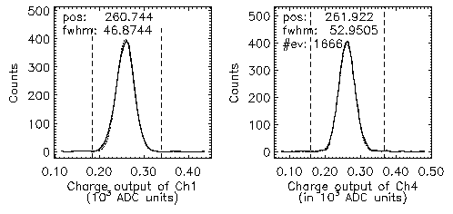
Spectra accumulated with the channels connected to junction 34 while illuminating the array with 500 nm (2.5 eV) photons. The plots include the fits used for calculating the resolution.
A partial matrix readout array has been created using a 6X6 Tantalum array to which a 4-channel data acquisition system was connected. Two channels (1 and 2) were used to bias and read the middle two lines while the other two channels (3 and 4) were connected to the middle two columns. The other four lines were biassed at a fixed voltage while the four remaining columns were grounded (see Martin et al 2000 for more details). Importantly, the array was able to be satisfactorily biassed and was stable during normal operations.
As an example of the results from this prototype, we show (above) two output spectra. For each junction, events were retained by selecting those which had a non-zero signal in both its corresponding channels, within a coincidence window of 5 microseconds. Further tests (below) were made to establish the degradation in energy resolution associated with the matrix scheme (see Martin et al 2000 for more details). The resolution of the matrix array is improved slightly by adding row and column signals.
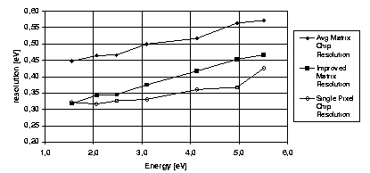
Comparison of energy resolutions between matrix-readout and conventional readout arrays.
Conclusions
Matrix readout is a novel connection scheme for pixelated detectors, drastically reducing the number of wires and associated circuits needed for reading out large array detectors. The devices can be properly biassed and show good spectral resolution, with energy resolutions only ~ 10% worse than those obtained using individual pixel readout.