X-ray DROIDS
 |
|
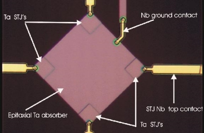
A Nomarski image of a 2-D DROID, with four STJ's arranged at the corners of an epitaxial Ta absorber |
DROIDS, Distributed Read-Out Imaging Devices, are one possible solution to this problem in both the X-ray and optical regimes. In a DROID, photons are absorbed in a single, large-area crystal (or a smaller polycrystalline layer), at the corners or edges of which are situated individual STJ's. Time-coincident event measurement allows the energy and position of an incoming photon to be reconstructed. The DROID therefore behaves similarly to a conventional large-area array of STJ's, at the possible expense of some energy resolution and the requirement to sustain a low count rate.
The Detectors and Optics group has been investigating the viability of 1- and 2-dimensional DROIDS as prototypical astronomical X-ray detectors, with the emphasis on spatial and energy resolution. The group's work on the feasibility of such devices as optical/UV detectors is summarised here, while matrix readout, another approach to the large-area format problem, is covered here.
Experimental set-up: Image Reconstruction
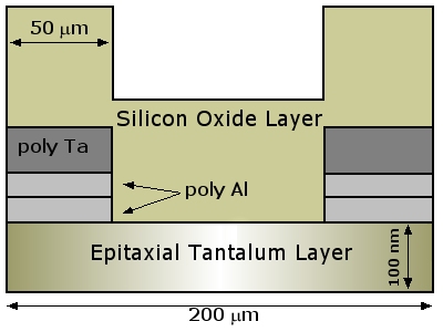
The 1- and 2-dimensional droids consist (see cross-section below) of an epitaxial Ta absorber with a thickness of 100 nm and an RRR of ~48, deposited on a sapphire substrate. The STJ's are symmetrical, with 100 nm thick Ta layers and 55 nm thick Al trapping layers. The base electrode is common with the absorber. To prevent oxidation, the whole detector is covered with a 480 nm thic SiOx layer. The STJ's have individual Nb connections to their top electrodes and a common Nb return contact via the absorber, intended to avoid quasi-particle losses through out-diffusion into the electrical connections. The junctions have a normal resistance of ~4.2 microOhms per square centimeter, with a gap energy of 0.42 meV.
 |
|
A cross-sectional sketch of a DROID, omitting the top-lead connections and the ~1.5 nm thick AlOx between the layers. The colour gradient in the absorber illustrates the change in energy gap from absorber to junction, due to the proximisation of the absorber by the first Al layer in the junction |
Three 1-dimensional and two 2-dimensional DROIDS were tested, and details of the absorber and STJ sizes of these individual devices may be found in Hartog et al (2000). In the first series of experiments the DROIDS were illuminated with a 55Fe source (producing emission features at 5.9 and 6.5 keV), with the devices contained in a ³He cryostat at a base temperature of 320 mK. The second and third series of tests were performed in collaboration with the Physikalisch-Technische Bundesanstalt (PTB) in Berlin, using the PTB SX-700 beamline at the BESSY I synchroton facility and the PTB FCM beamline at BESSY II. BESSY I offers photons in the range ~40 eV to 1.95 keV, while BESSY II runs from 1.7 to 11 keV. Details of subgap currents and bias voltages in these tests may be found in Hartog et al (2000) , together with details about the read-out modes of the STJ's.
Image Reconstruction
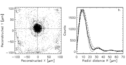
An incoming photon hitting a 2-D DROID somewhere in the absorber will produce coincident signals in the four corner STJ's. How do we reconstruct the (x,y) coordinates of the event from the coincident charge signals? In order to do so, we need to define a model that predicts the charge signals as a function of (x,y), and then invert this model to derive event positions for our list of measured coincident charge signals. The model has to take into account qp diffusion, losses and tunneling, as well as the characteristics of the pulse-processing electronics. It turns out to be quite easy to construct such a model based on numerical finite-difference technqiues, but in order for the model to supply useful spatial resolution, exceedingly large computational resources are needed. Further details are found in Hartog et al (2000), but as an example of a reconstructed image, we show the illumination of a DROID with a Fraunhofer diffraction pattern (see below):
 |
|
A Fraunhofer diffraction pattern created with 10 keV photons through a 5 micron pinhole at 650 mm in the Bessy II synchrotron facility (left), and (right), the radial average of the pattern compared with the theoretical pattern (dotted line), and the theoretical pattern after convolution with a gaussian point-spread functrion (PSF) of width 12 microns (dashed line) and 7 microns (solid line) |
Energy Resolution
A number of factors currently complicate the determination of the energy resolution of 2-D DROIDS, so we here restrict our discussion to one-dimensional devices. The analysis of data from 1-D DROIDS is clearly simpler, but there are still several complications.
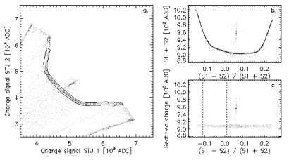
It is found that when the signal from one STJ is at maximum, the signal from the other is still ~ 60% of its maximum value, indicating that quasi-particles are hardly trapped in our STJ's. Another complicating factor is that the shape of the current pulses generated in the STJ's depends on absorption position. This means that a single shaping filter cannot be optimized for all the different pulse shapes, requiring us to correct for the differences in charge output. The steps involved are outlined in the figures below.
 |
|
The first three data reduction steps in the computation of the energy resolution of a 1-D DROID. The data were obtained at the PTB FCM beamline at an energy of 5895 eV, allowing direct comparison to spectra obtained with a 55Fe source. The leftmost figure shows a scatter plot of the charge signals from the two STJ's against each other, with the border indicating the selected absorber events. The upper rightmost plot shows the transformation to a plane in which the x-axis corresponds roughly with position in the absorber, and the y-axis with the total charge of the event. The fit is a high-order polynomial, which is used to correct for the variations in charge output with position. The lower plot on the right shows the corrected charge output as a function of the equivalent of position in the absorber, with the dashed vertical lines indicating the selection of events for the determination of the energy resolution. |
The energy resolution of a DROID is determined by three essentially Poissonian processes, their contribution to the resolution scaling with the square root of the photon energy:
 |
where the three terms F,G and H in the above equation are:
- Fano limit: This fundamental limit to the energy resolution is set by the statistical noise on the number of quasi-particles created after the absorption of a photon. The limit is independent of the design of any detector which depends on the detection of charge. The Fano factor, F, was calculated to be 0.22 for photons of a few eV in Niobium, a figure that we currently assume to be reasonable for other photon energies/materials.
- Tunnel limit: Statistical fluctuations in the tunnelling of quasi-particles in STJ's introduces another factor, G.
- Cancellation Noise: Quasi-particles with energies above a certain threshold may tunnel in a way that reduces the tunnel current. These are events that correspond to two terms in the tunnelling Hamiltonian that are usually ignored. Statistical fluctuations on this process give rise to the cancellation noise, H, which may give significant contributions for very low bias voltages (low threshold), or in the case of incomplete relaxation of the quasi-particle population.
There are several other statistical contributions which only apply to DROIDS which (unlike ours) operate in the strong-trapping regime. In addition, there are also electronic noise and bias instability contributions to the overall resolving power degradation. The first term may be subtracted from the total noise by reference to test pulser observations.
Finally there are contributions from variations of quasi-particle losses with absorber position, both along the width and length of the absorber. Details on the modelling of the energy-resolution may be found in Hartog et al (2000). The table below displays the best measured energy resolutions at several energies against the expected contributions from the various mechanisms discussed above, with the various discrepancies (and likely explanations) again discussed in Hartog et al.
| FWHM Resolution (eV) | ||||
| Photon Energy | 1000 eV | 3500 eV | 5895 eV | 10 keV |
| Measured | - | 13.3 | 16.9 | 30.0 |
| Pulser | - | 5.8 | 7.1 | 12.0 |
| Intrinsic | 6.3 | 12.0 | 15.3 | 27.5 |
| Fano Limit | 1.2 | 2.3 | 2.9 | 3.8 |
| Tunnel Noise | 2.7 | 5.1 | 6.6 | 8.6 |
| Cancellation Noise | 0.3 | 0.6 | 0.8 | 1.0 |
| Recombination | 0.9 | 4.6 | 9.0 | 28.8 |
| Total | 3.0 | 7.3 | 11.6 | 30.3 |
Requirements for Large-format Detectors
If DROIDS are to be flown on future space missions, they will need to be increased in size such that they have absorber dimensions of several mm. The tunnel noise is the main limiting factor; increasing the length of the absorber while keeping the STJ's at the same size decreases the barrier area and hence tunnel probability, and thus raises the tunnel noise. Scaling up the STJ's increases their capacitive noise. Moving to lower energy-gap materials such as Hafnium improves the quasi-particle statistics, but the time resolution must be improved by a factor of 10 before it reaches the < 5 microsecond level required by a mission such as XEUS. This may be achieved by decreasing the impurity content of the absorber (see Hartog et al (2000) for more details).
