Solar Electron Proton Telescope (SEPT)
Introduction
| This page has been archived and is no longer updated. |
The SEPT instrument presently operates on board the STEREO mission as part of the IMPACT (In-situ Measurements of Particles and CME Transients) suite of instruments within the SEP (Solar Electron Proton) package. SEPT consists of two dual, double-ended magnet/foil solid state detector particle telescopes that cleanly separate and measure electrons in the energy range 20-400 keV and protons from 60-7000 keV, while providing anisotropy information through use of several fields of view.
 |
|
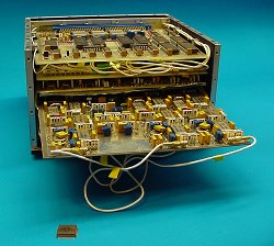
Figure 1: The PDFE chip (on the bottom) is compared here with the discrete development used for previous missions, in that case an instrument on board WIND. The PDFE integrates the functionalities standing on one and a half of the presented board. |
Two SEPT units (NS: North-South direction, E: Ecliptic) are located on each STEREO spacecraft. The electronics were provided by ESA-ESTEC, SCI-A. The housing and the sensors were provided by the University of Kiel (Germany).
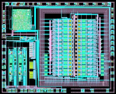
The major challenges of SEPT follow the growing need of compact and highly integrated instruments. SEPT is based on an ASIC (Application Specific Integrated Circuits) developed for the Space Science Dept. of ESA under it's GSTP program: PDFE (Particle Detector Front End).
With 640 g and 600 mW per SEPT unit, the instrument prevails the technological development which will have to be performed to respond to the future always more demanding space mission (see Figure 1).
Overview
| This page has been archived and is no longer updated. |
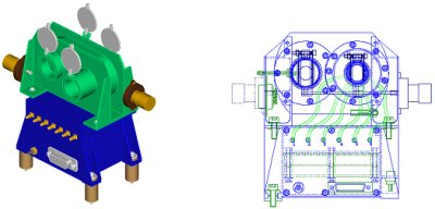
The structure of the instrument consists of two parts: the electronic box, containing 3 boards and the sensor head with the two telescopes, one telescope containing one pair of detectors. Each PIPS (Passivated Implanted Planer Silicon) detector consists of one centre segment surrounded by a cross-talk ring and a guard ring and is 300 μm thick.
 |
|
Figure 2: On the left, a 3-D view of one SEPT unit with its open protection covers. On the right, detailed view of the SEPT showing the structure of the sensor head and the 3 boards, from top to bottom: analogue/EMI shied/digital (Drawings courtesy Uni. of Kiel) |
| Description | Goal |
| F.O.V. |
2 sets for electrons and protons, each with: 2 opposing view cones in ecliptic, 2 opposing view cones off-ecliptic, 52° full opening angle |
| Energy |
20 - 400 keV electrons 60 - 7000 keV protons |
|
Energy Resolution (Telemetry) |
20% electrons 20% protons |
| Geometric Factor |
0.52 cm²steradians electrons 0.68 cm²steradians protons |
| Background | <0.2 counts/s on ground, 20 °C |
| Max Event Rate |
25 000 counts/s at 2.2 MeV 250 000 counts/s at 55 keV |
| Time Res. Science | 60 s |
| Time Res. Beacon | 60 s |
|
Allocated mass (without harness and per unit) |
640 g |
|
Allocated Power (average per unit) |
600 mW |
| Environmental Conditions |
operating temperature: -25 °C to +40 °C TID 12 krad (5 yr extended mission with 75 mil AI) |
Electronics
| This page has been archived and is no longer updated. |
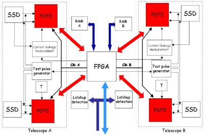
Each detector is connected to one PDFE. The control of the four PDFEs, together with the interface to the central processor of the SEP package is managed by an ACTEL RT54SX32S FPGA. The analog electronics is divided into two totally independent parts as shown on the diagram above (one for each telescope). The PDFEs are also used as A-to-D converter for temperature and detector leakage current measurements. A pulse generator (one per telescope) can be used to check the front-end electronics during flight.
 |
|
Figure 3: Electronics block diagram |
 |
|
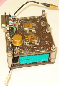
Figure 4: View of the board stack (at the top the back of the digital board with two SRAMs) |
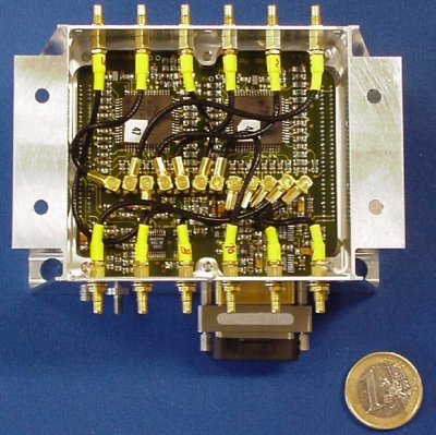
The highly populated stack of 3 boards (analog board, digital board and EMI shield) is placed within the instrument base box. The different signals are routed from the detectors to the sidewall of the box via coax cables and then from the sidewall of the box to the analog board.
To gain in the integration of the electronics and as a growing trend, it was decided to use commercial parts for functionalities evaluated as non-critical and when no military or space-qualified equivalent was available. Hence, five parts (ADG704, ADG713, MAX892, ADP3300, TLC2262) were up-screened and together with the PDFE went through radiation testing. Total Ionizing Dose and heavy ions were studied at ESTEC (D/TOS-QCL) and have shown compliance with the mission constraints (12 krad with 75 mil Al for the 5 years extended mission). The potential latch-ups due to heavy ions are addressed thanks to a dedicated mitigation technique, also successfully tested at ESTEC.
 |
 |
|
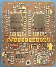
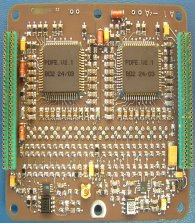
Figure 5: Views of the top and bottom side of the analog board (Flight model) |
|
 |
|
|
Figure 6: View of the top of the analog board with the internal cables in the electronic box (Engineering model) compared to a one-euro coin |
|
PDFE
| This page has been archived and is no longer updated. |
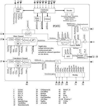
The PDFE is suited for charged particle spectroscopy applications. It contains two analog charge-amplifying channels. The first channel is the main one, whereas the second channel is used for coincidence (or gating) purposes. Coincidence means that when two external detectors are placed close to each other, the events resulting from the penetration of particles through the first detector are inhibited by their detection by the second detector or, contrary, do require a detection by the second detector. The coincidence detection can also be done externally; a digital input is provided as coincidence input. Eight-bit-programmable discriminators are provided for both channels. A peak detector holds the peak value of the main semi-gaussian pulse. An 8-bit analog-to-digital converter is implemented on chip to digitize that peak value.
A cascadable serial link is used to observe and control one or several PDFEs. The main four modes of operation are the following:
- Charge amplification mode (main channel active only, external gating)
- Coincidence detection mode (both channels active, second channel used for gating)
- Charge amplification mode with active coincidence channel (both channels active, external gating) A-to-D conversion mode (the PDFE acts as a simple A-to-D converter)
The detailed characteristics are the following:
- Two charge amplifying channels
- Built-in 8-bit discriminators
- Linear 8-bit ADC
- Completely event-driven
- All internal registers SEE protected
- Package 64 pin CQFP (Ceramic Quad Flat pack)
- Maximum detector capacitance: 100 pf
- Maximum detector leakage current: 0.1 pC
- Minimum detection charge: 0.37 fC
- Conversion gain: 30mV/fC
- Conversion gain adjustment: +/- 5%
-
Noise: 740 erms or 6.3 keV FWHM at 0pf (measured)
1160 erms or 9.8 keV FWHM at 120 pf (measured) - Noise slope: 4.2 erms/pf
- Peaking time: 1 µs
-
Maximum counting rate: 250 ksamples/s at maximum detection charge/40
25 ksamples/s at maximum detection charge - Maximum pulse amplitude at 3 V analog output
The PDFE is the result of a collaboration between:
- ESA/ESTEC: S. Habinc, B. Johlander, T. Sanderson
- KULeuven, ESA-MICAS: G. Gielen, J. Vandenbussche, G. Van Der Plas
- IMEC, Invomec: C. Carl Das, K. Marent, S. Redant, J. Wouters, D. Lambricht.
 |
|
Figure 7: PDFE Block Diagram |
 |
|
Figure 8: Structure of the PDFE die (actual size 5 mm × 6 mm). The PDFE was developed and manufactured by IMEC with the 0.7 mm Mietec CMOS process |
Preliminary results
| This page has been archived and is no longer updated. |
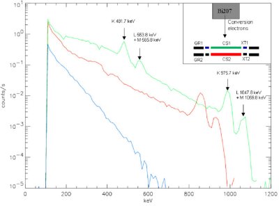
The PDFEs were operated in full anti-coincidence. The green curve is related to CS1, the centre segment of D1. The red curve shows the fluence observed on CS2, the centre segment of D2. The blue curve is related to XT1, the cross-talk ring of D1. On the top right, a basic sketch of the position of the source with respect to the detectors is represented. The K conversion lines are nicely resolved. The different lines are also visible on CS2, shifted by ~110 keV, the average energy deposited by electrons which cross D1.
 |
|
Figure 9: The first spectra obtained with the breadboard model of one telescope and the dedicated electronics, using the electron conversion lines of a Bismuth 207 source |
The Engineering Model has undergone successful interface tests in Caltech in June 2003 and will be used with the flight detectors in August. The four SEPT flight models (plus one spare) are now assembled and will be delivered in December 2004 after environmental and EMC tests and calibration campaign.
Flight Model
| This page has been archived and is no longer updated. |
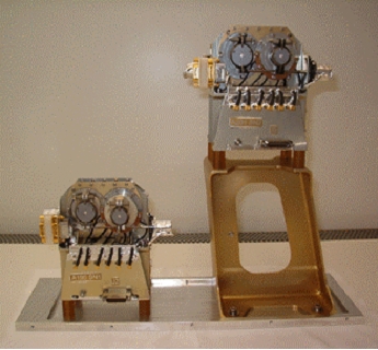
After successful environmental testing and calibration, the four SEPT units (see figure 9) have been integrated on the twin observatories.
 |
|
Figure 9: Two of the four flight units (SEPT-E and SEPT-NS) |
The two STEREO spacecraft were successfully launched on 26 October 2006, at 00:52 UTC (20:52 EDT, 25 October) on a Delta II 7925-10L rocket from Cape Canaveral Air Force Station in Florida.
Following a series of Earth-Moon fly-bys, the two spacecraft reached their science orbit about three months later in late January 2007. One spacecraft (STEREO-A) orbits ahead of Earth in its orbit around the Sun, while the other spacecraft (STEREO-B) trails behind Earth. The separation between the two spacecraft progressively increases at a rate of ~44° per year as viewed from the Sun.
First Results
| This page has been archived and is no longer updated. |
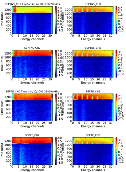
During the different Moon-Earth fly-bys the SEPT sensors, as well as the other instruments of the IMPACT consortium, have successfully been commissioned. During this period two events of particular importance took place:
|
14 December 2006 All eight SEPT doors on STEREO-A(head) fully open |
||
| 17:32 UT | SEPT-NS | Proton & electron apertures viewing north |
| 17:45 UT | SEPT-E | Proton & electron apertures viewing anti-Sun |
| 17:57 UT | SEPT-NS | Proton & electron apertures viewing south |
| 18:10 UT | SEPT-E | Proton & electron apertures viewing towards Sun |
 |
||
|
Figure 10: SEPT Raw data for 14 December 2006 on STEREO-A. The horizontal axis corresponds to the energy channel and the vertical axis to the time in minutes (1440 minutes of a full day). The colour coding is in log10 scale in counts/minute. Last measurement occurred at 23h49m49s. On NS-CH1, NS-CH3, E-CH1 and E-CH3, a pattern is clearly visible. This is due to a minor mistake in the compression algorithm of the impact processor software and will require a software patch. |
|
16 January 2007 All eight SEPT doors on STEREO-B(ehind) fully open |
||
| 20:32 UT | SEPT-NS | Proton & electron apertures viewing south |
| 20:43 UT | SEPT-E | Proton & electron apertures viewing towards the Sun |
| 20:55 UT | SEPT-NS | Proton & electron apertures viewing north |
| 21:06 UT | SEPT-E | Proton & electron apertures viewing anti-Sun |
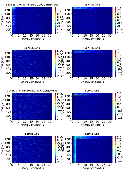 |
||
|
Figure 11: SEPT Raw data for 16 January 2007 on STEREO-B. The horizontal axis corresponds to the energy channel and the vertical axis to the time in minutes (1440 minutes of a full day). The colour coding is in log10 scale in counts/minute. |
