Plasma Jet Machining on strongly curved off axis parabolic SiC mirrors
Date: 19 June 2009
Satellite: Gaia
Copyright: TNO/IOM/Fred Kamphues
TNO Science and Industry and the Leibniz Institute of Surface Modification (IOM) are developing processes for finishing strongly curved off axis parabolic silicon carbide (SiC) mirrors. The mirrors form a crucial part of the cryogenic fibre collimators for the Gaia Basic Angle Monitoring Opto-Mechanical Assembly (BAM OMA).
The Gaia BAM OMA is a double Michelson interferometer which measures the basic angle between the two telescopes with an accuracy of better than 0.5 microarcseconds. The Gaia BAM OMA consists of two SiC optical benches with fibre collimators, beam splitters and a large number of folding mirrors.
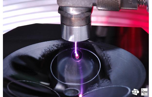
The off axis parabolic SiC mirrors are designed by TNO in close cooperation with Astrium and were manufactured by Boostec. TNO and IOM use a combination of 3D robot polishing and Plasma Jet Machining (PJM). Plasma enhanced chemical etching is a non-conventional technology for surface machining. The method is based on a microwave or RF excited plasma jet under normal atmospheric pressure or in rough vacuum yielding a high flux of reactive radicals. Material removal is obtained by chemical reactions between the radicals and surface atoms.
Different plasma jet sources have been developed to do deterministic surface shaping and surface figure error correction over a wide spatial range with nanometre accuracy. The half-width of the almost nearly Gaussian like shaped removal functions reaches from about 0.1 mm to about 10 mm. Maximum volume removal rates of about 50 mm³ per minute have been achieved for fused silica and ULETM. Surface machining is accomplished using the dwell time algorithm on CNC controlled multi-axes systems. Far developed mathematical de-convolution routines are used for creating the machining files.
During plasma jet treatment no sub-surface damage occurs in contrast to abrasive methods. This advantage makes the plasma jet technology very attractive for the precise manufacturing of especially spherical and free-form optics. On the other hand the chemical removal mechanism leads to an increase of surface roughness depending on the material and the removal depth. But at the same time potential subsurface damage is removed. A low surface roughness is achieved with a post polishing run on the Zeeko polishing robot at TNO.
The parabolic mirror is made of silicon carbide (SiC) and needs to be polished to a surface error of less than 12.5 nm RMS. The main difficulty of this mirror is its small radius of curvature (R = 50.17 mm) over an effective aperture of 10 mm. During trial runs by IOM and TNO a surface error of 8 nm RMS was achieved. Production of the flight mirrors has started.
More information can be found on:
http://www.tno.nl/gaiabam
http://www.iom-leipzig.de/html/eng/nachwuchsforschergruppe_uat.cfm