Compound Semiconductors
 |
Semiconductor materials have already been used in alpha, proton and X-ray spectroscopy, in both remote and direct sensing experiments. However, while remote sensing missions have studied the moon, they suffer from limited sensitivity and crude spatial resolution. This is because, up till now, planetary science has lacked short focal length optics matched to a thin but highly absorbent detection plane, which for interplanetary missions must also be free of the power, weight and cryogenic constraints normally associated with traditional detection technologies. New developments in slumped micro channel plate technology and wide band-gap compound semiconductors offer the potential of circumventing these problems, providing spatially resolved, Fano limited spectroscopy across the energy range 1-200 keV.
What are compound semiconductors?
The term compound semiconductor encompasses a wide range of materials, most of which crystallize in either the zincblende (ZB), wurtzite or rocksalt crystal structures. They were first investigated as radiation detectors in 1945 by Van Heerden, who demonstrated that silver chloride crystals when cooled to low temperatures were capable of detecting γ-rays, α-particles and β-particles. This work was later extended to the thallious halides by Hofstadter in 1949. Strangely, at this time, the elemental semiconductors were not anticipated to be responsive to radiation and it was not until several months later than McKay managed to measure the polonium α-ray spectrum using a Ge surface barrier detector. While the subsequent development of Ge and Si radiation detectors was rapid, largely due to the explosive rise of the semiconductor industry, mixed-element and compound semiconductors, such as the alkali-metal halides, CdTe, CdZnTe and HgI2, were plagued by material problems caused by severe micro-crystallinity, high defect densities, impurities and stoichiometric imbalances. Until the 1960s very little additional work was carried out. Since this time, progress has been incremental, but hardly spectacular.
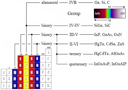 |
Compound semiconductors are generally derived from elements in groups II to VI of the periodic table. They are so useful because of the shear range of compounds available, compared to the elemental semiconductors, Sn-α, C, Si and Ge. Most elements in these groups are soluble within each other, forming homogeneous solid solutions. These solutions occur when atoms of a particular element are able to substitute a given constituent of a different material without altering its crystal structure.
 |
|
Alloying: atoms mixed on a lattice - Solid Solutions and Ordered Compounds. |
In order that atoms can form solid solutions over large ranges of miscibility, they should satisfy the Hume–Rothery Rules, namely that,
- they have comparable atomic radii (differ by < 15%) allowing substitution without large mechanical distortion,
- individually, their crystal structures are the same,
- the two species have similar valences, and
- their electronegativities are similar to avoid the creation of inter-metallic compounds.
The rationale behind the Hume-Rothery Rules is:
- Atomic radii must be similar because if the substituted atom is too large, considerable strain will develop in the crystal lattice.
- The components must have similar crystal structure if solubility is to occur over all proportions, e.g., in the Co/Ni system. However, this is less important if small proportions of a solute are being added such as in the doping of semiconductors.
- Similar valences and electronegativities indicate that components have similar bonding properties.
In addition to binary materials (such as GaAs or InP), most compounds are also soluble within each other, making it possible to synthesize ternary (e.g., AlGaAs, HgCdTe) quaternary (e.g., InGaAsP, InGaAlP) and higher-order solutions, simply by alloying binary compounds together.
Why use compound semiconductors?
Apart from its on-going development of micro channel plate optics, the Advanced Technologies Section is studying the suitability of several compound semiconducting materials, including GaAs, CdZnTe, TlBr, InP and HgI2. These all have band-gaps sufficiently high so they do not require cryogenic cooling but low enough that sub-keV spectral resolution may be achieved at hard X-ray energies. In addition, the materials are drawn from group III and V compounds and so have high enough atomic numbers to ensure high detection efficiencies above 10 keV.