Compound Semiconductor Growth Facilities
To support the Offices' extensive compound semiconductor program, a number of external growth facilities have been set-up. The reasons for this are purely practical, to support the PIs and Project in the procurement of difficult-to-get materialto secure the supply chain for the project duration to be able to influence the growth process to improve material quality
Cadmium Telluride and Cadmium Zinc Telluride
 |
|
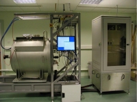
Installation at Durham Scientific Crystals Ltd, England |
Growth Facilities to produce both CdTe and CdZnTe have been set up at Durham Scientific Crystals Ltd in Durham England as part of ESAs Industrial Triangular Initiative program. The Company has pioneered the Multi-Tube Physical Vapour Transport Method to produce binary and ternary II-VI compounds. This technique has distinct advantages over conventional High Pressure Bridgeman (HPB) in that it separates the source and growth regions of a vapour transport system into separate vertical furnaces connected by a horizontal transport tube. The transport passage incorporates a flow restrictor which regulates the mass flow and decouples it from the source-sink temperature difference. Growth takes place on a seed crystal past which the growth envelope is dynamically pumped to ensure that the transport is diffusion-less. This "multi-tube" arrangement offers several advantages over conventional linear vapour transport systems. In addition to the fine control of the mass transport, source and growth regions are thermally decoupled and therefore both regions can be monitored in-situ and non-invasively. Also precisely because the growth region is decoupled, there is much greater control of the nucleation and subsequent growth of large single crystals of high-vapour pressure opto-electronic materials such as the II-VI compounds. In essence, this process has the potential of producing large single crystal yields with good stoichiometry, at a high growth rate and at a fraction of the cost of HPB. The kit is illustrated on the right and has just undergone commissioning trials. The results were very favourable.
Cadmium Manganese Telluride
Durham Scientific Crystals Ltd has also set up a small research reactor to produce CdMnTe - funded by SCI-A. The goals of the CdMnTe programme are:
-
 |
|
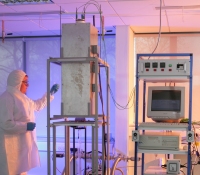
Installation at Durham Scientific Crystals Ltd, England |
To produce cadmium manganese telluride single crystals using the MTPVT method. The crystals will be grown using binary starting materials. The work will be carried out in a custom built crystal growth system which would be capable of growing small pieces (0.125 - 0.5 cm³) of single crystals of cadmium manganese telluride for proof of concept work. The process however can be scaled up to produce significantly larger crystals (10 cubic cm) beyond this stage
- To produce a range of composition of the crystals, which will be characterised to verify the composition, crystalline quality and electrical resistivity. The programme will produce crystals with manganese content (x in Cd1-xMnxTe) ranging from 0.05 to 0.15
The kit is shown above. At present the gas-flow transport rates and being quantified as a function reactor temperature
Thallium Bromide
 |
|
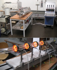
Installation at Korth Kristalle in Kiel, Germany |
Thallium bromide is grown at Korth Kristalle in Kiel Germany. The TlBr is grown by the floating zone technique which can produce cylindrical boules up to 40 mm in diameter and some 10 cm long. This technique is similar to zone refining, which is actually carried out first in multiple passes to purify the raw materials before going into the floating zone furnace. Floating zone growth relies on the fact that the segregation coefficient k (or, the ratio of an impurity in the solid phase to that in the liquid phase) of most impurities in TlBr is less than unity and therefore when molten liquid TlBr is in contact with solid TlBr, the impurity atoms will tend to diffuse to the liquid region. Thus, by passing a boule of TlBr through a thin section of furnace very slowly such that only a small cylinder of the boule is molten at any time, the impurities will collect in the molten region and migrate with it as the boule is moved through the heat zone. Because of the lack of impurities in the leftover regions which solidify, the boule can grow as a perfect single crystal if a seed crystal is placed at the base to initiate a chosen direction of crystal growth. The image on the right gives two views of the facility - top: the floating zone growth setup, bottom: testing the zone heaters.
Boron Carbide
 |
|
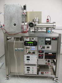
Installation at Cambridge MicroFab Ltd in Cambridge, England |
Boron carbide is grown by the Plasma Assisted Chemical Vapour Deposition (PACVD) at Cambridge MicroFab Ltd in Cambridge England. The system is a parallel-plate PACVD reactor designed to be used with either decaborane (B10 H14) or orthocarborane (C2B10H12) vapour as the main reactant gas, and optionally methane as a second reactant gas. Argon is used as the carrier gas for the vapours and the ballast gas for the plasma. The precursor is kept in a temperature-controlled pot near the chamber and its rate of consumption is controlled by the argon flow through the pot, as well as by temperature. The substrate can be either 2 inch or 50 mm in diameter. It can be heated up to a temperature of at least 850 °C and is loaded via a load lock chamber. In order to obtain a uniform gas mix over the wafer, the precursor vapour is fed through the RF electrode. The methane and ballast argon gas are fed through the substrate heater. It is also possible to reconfigure the system by fitting a magnetron instead of the RF electrode, so as to have a reactive sputtering system. The system is enclosed in an oven, in order to inhibit the condensation of toxic compounds on the walls. It also makes the system easily bakeable.
Last Update: 1 September 2019
