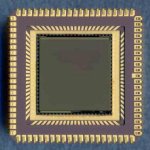
Active Pixel Sensor
As far as spectral response is concerned, the UV range is only at the exploration phase, with the application of CCDs "recipes" like specific coating deposition. Backside illumination technology, already applied to CCDs, is one way to extend the spectral coverage of APS. Another very promising alternative is the hybridation of the readout architecture to specific substrate with targeted optical properties (such as Wide Band gap semiconductors), with the possibility as stated earlier, to optimize them separately.
Imaging payloads of the future ESA missions such as Bepi Colombo and Solar Orbiter could largely benefit from progress of the APS technology. Within that frame and as part of the 2004-2006 TRP (Technology Research Program), SCI-A is managing the following activities:
- A 2048 x 2048 Active Pixel Sensor with improved radiometric performances for the visible imagers of the Bepi Colombo MPO (Magnetospheric Planetary Orbiter). The extension toward UV by suitable techniques should also profit to the Solar Orbiter imaging payload.
- A 256 x 256 focal plane array based on APS for the NIR (0.5 to 2.5 μm) for the Bepi Colombo Near Infrared Imaging spectrometer. The use of HgCdTe substrate is a very strong option.
 |
|
Star1000 chip - a 1000 x1000 pixel chip has a 15 um pixel size. |
- A monochromator (Cornerstone CS130) and integrating sphere setup to evaluate PRNU (Photo Response Non Uniformity, Gain, Spectral response, Quantum efficiency, Fill Factor
- A micrometer size laser spot setup to evaluate pixel cross talk, pixel profile, PSF (Point Spread Function) and eventually MTF. The use of a USAF target is also foreseen
- Calibrated Radiometer
- High accuracy positioning system to perform the above mentioned operation
The test bench will operate typically from 300 nm up to 2 μm.
